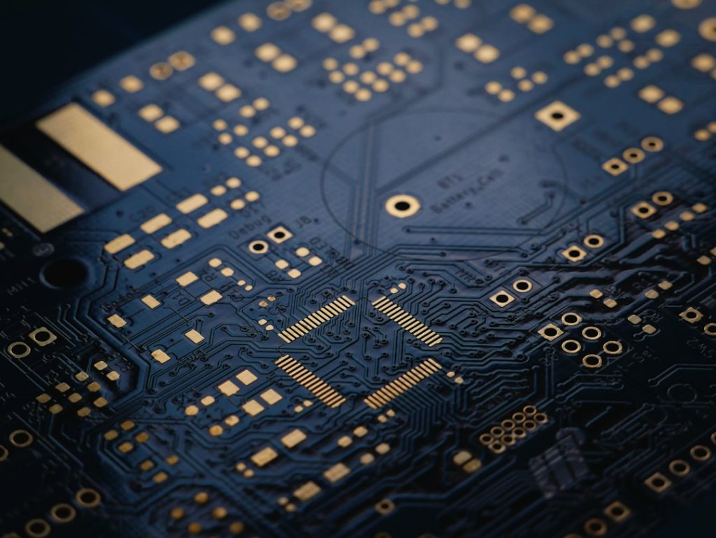
Modern electronics depend on printed circuit boards that are assembled with precision, consistency, and careful quality control. In a typical manufacturing environment, PCB assembly moves through a structured workflow that transforms a bare board and a set of components into a functional electronic product ready for integration, shipment, or further system-level testing.
TLDR: PCB assembly begins with design review and material preparation, then moves through solder paste application, component placement, soldering, inspection, and testing. Each stage helps ensure that components are accurately installed and electrically reliable. Final testing confirms that the assembled board performs as intended before it leaves the production line. A strong workflow reduces defects, improves repeatability, and supports scalable manufacturing.
Preparing for PCB Assembly
Before any component is placed, the manufacturer must verify that the project files, materials, and process requirements are complete. This preparation stage usually includes reviewing the bill of materials, Gerber files, pick and place data, assembly drawings, and test requirements. If a board has design issues, component shortages, or unclear placement instructions, problems can spread throughout the entire production run.
The engineering and production teams typically perform a design for manufacturability review. This review checks whether the PCB layout is suitable for automated assembly, soldering, inspection, and repair. Common concerns include component spacing, pad geometry, thermal relief, polarity markings, and access for test probes. Addressing these issues early can prevent costly rework later.
- Gerber files define the copper layers, solder mask, and silkscreen.
- BOM data identifies every required component and manufacturer part number.
- Pick and place files guide automated machines during component placement.
- Assembly drawings show orientation, polarity, and special handling notes.

Material Sourcing and Incoming Inspection
Once documentation is approved, materials must be sourced and inspected. This includes bare PCBs, resistors, capacitors, integrated circuits, connectors, mechanical parts, and any special hardware. Reliable sourcing is essential because counterfeit, damaged, or incorrectly specified components can compromise the final product.
Incoming inspection may involve checking labels, date codes, moisture sensitivity levels, packaging condition, and component values. Bare boards may be examined for surface defects, plating quality, solder mask alignment, and dimensional accuracy. Components that are sensitive to moisture are often stored in controlled environments or baked before assembly to prevent damage during reflow soldering.
Solder Paste Application
For surface mount technology, the first major production step is usually solder paste printing. Solder paste is a mixture of tiny solder particles and flux. It is applied to the PCB pads through a stainless steel stencil. The stencil has openings that match the pads where components will be soldered.
This step is critical because many assembly defects originate from poor solder paste deposition. Too much paste can cause bridging between pins, while too little paste can create weak or open joints. Manufacturers often use automated solder paste inspection to measure paste height, area, volume, and alignment before components are placed.
Key variables in solder paste printing include:
- Stencil thickness: Controls paste volume for different component types.
- Squeegee pressure: Affects how evenly paste fills the stencil apertures.
- Print speed: Influences paste release and consistency.
- Board support: Prevents movement or flexing during printing.
Component Placement
After solder paste has been applied, the board moves to component placement. Automated pick and place machines use feeders, nozzles, vision systems, and placement data to position components onto the pasted pads. These machines can place thousands of components per hour with remarkable accuracy.
Small passive components such as resistors and capacitors are usually placed very quickly, while larger integrated circuits, BGAs, connectors, and fine-pitch devices require more controlled handling. The machine verifies component orientation and position before placement. Proper programming is essential, especially for polarized parts such as diodes, electrolytic capacitors, LEDs, and ICs.

During this stage, production staff may monitor feeder setup, component replenishment, nozzle condition, and machine calibration. For prototype or low-volume builds, some parts may be placed manually, especially odd-shaped components that cannot be handled efficiently by automated equipment.
Reflow Soldering
Once components are placed, the PCB passes through a reflow oven. The oven follows a temperature profile designed to gradually heat the board, activate the flux, melt the solder particles, form solder joints, and cool the assembly in a controlled manner. A well-developed reflow profile helps prevent defects such as tombstoning, solder balls, cold joints, and component damage.
The reflow process generally includes four phases: preheat, soak, reflow, and cooling. During preheat, the board temperature rises gradually to reduce thermal shock. During soak, temperatures stabilize and flux removes oxides from soldering surfaces. In the reflow phase, solder melts and forms metallurgical bonds. Finally, cooling solidifies the joints.
Different assemblies may require different profiles depending on board thickness, copper weight, component size, solder alloy, and thermal sensitivity. Lead-free solder, for example, usually requires higher peak temperatures than traditional tin-lead solder.
Through Hole Assembly and Wave Soldering
Not all components are surface mount devices. Some assemblies include through hole parts such as connectors, transformers, switches, relays, and large capacitors. These components have leads that pass through holes in the PCB and are soldered on the opposite side.
Through hole components may be inserted manually or with automated insertion equipment. After insertion, the board may go through wave soldering, selective soldering, or hand soldering. Wave soldering exposes the underside of the PCB to a wave of molten solder, while selective soldering targets specific joints with greater precision. Hand soldering is often used for prototypes, repairs, or components that require special handling.
Inspection After Soldering
Inspection is essential after soldering because even a well-controlled process can produce defects. Automated optical inspection, often called AOI, uses cameras and image processing to check for missing components, incorrect polarity, misalignment, solder bridges, insufficient solder, and lifted leads. AOI is fast and effective for visible components and solder joints.
For hidden joints, such as those beneath ball grid array packages, manufacturers may use X-ray inspection. X-ray systems can reveal voids, bridges, open joints, and alignment problems that cannot be seen from the outside. This is especially important for high-reliability products used in automotive, aerospace, medical, or industrial environments.

Cleaning and Conformal Coating
Depending on the solder paste and flux used, the board may require cleaning after soldering. Some no-clean fluxes are designed to remain on the board, but certain applications still require residue removal to improve reliability, appearance, or coating adhesion. Cleaning may be performed with aqueous systems, solvents, or ultrasonic equipment, depending on the materials involved.
Some assemblies also receive conformal coating. This thin protective layer helps shield the PCB from moisture, dust, chemicals, and temperature changes. Coatings may be applied by spraying, dipping, brushing, or selective coating machines. Before coating, sensitive areas such as connectors, test points, and switches may need to be masked.
In-Circuit Testing
After visual and structural inspections, electrical testing begins. In-circuit testing checks individual components and circuit connections while the board is still accessible at the PCB level. A bed-of-nails fixture or flying probe system contacts specific test points to measure resistance, capacitance, diode behavior, shorts, opens, and component presence.
In-circuit testing is particularly useful for finding manufacturing defects before power is applied to the full assembly. It can detect wrong values, missing components, solder bridges, and open connections. However, it requires good test access and may involve custom fixtures for higher-volume production.
Functional Testing
Functional testing verifies that the assembled PCB performs its intended operation. Instead of only checking individual parts, functional testing evaluates the board as a working system. Power is applied, signals are generated, firmware may be loaded, and outputs are measured against expected results.
Examples of functional tests include checking communication interfaces, sensor readings, voltage regulation, timing accuracy, display output, motor control, wireless performance, or current consumption. The exact test procedure depends on the product’s purpose. A power supply board, for instance, may be tested under different loads, while a communication module may be tested for data transfer and signal strength.
Functional testing is often the final proof that the assembled board is not only built correctly, but also capable of doing its job in real-world conditions.
Programming and Firmware Loading
Many modern PCB assemblies include microcontrollers, memory devices, or programmable logic. These parts may need firmware programming during or after assembly. Programming can be done through test pads, connectors, or dedicated programming fixtures.
After firmware is loaded, the board may undergo verification to confirm that the correct software version has been installed. This step is important for traceability and product consistency. In regulated industries, programming records may be linked to serial numbers and production batches.
Final Quality Control and Documentation
Before shipment, the PCB assembly goes through final quality control. This may include visual inspection, dimensional checks, label verification, packaging inspection, and review of test results. Boards that fail inspection may be sent to a repair station for rework and retesting.
Documentation is also part of the workflow. Manufacturers may record lot numbers, inspection results, test data, operator information, and process conditions. These records support traceability, warranty analysis, and continuous improvement. For critical applications, detailed documentation can be just as important as the assembly itself.
Packaging and Shipping
Completed PCB assemblies must be packaged to prevent electrostatic discharge, moisture exposure, and mechanical damage. Anti-static bags, trays, foam, and moisture barrier packaging are commonly used. If the boards are sensitive to humidity, desiccant and humidity indicator cards may be included.
Clear labeling helps identify part numbers, revisions, quantities, serial numbers, and handling requirements. Proper packaging ensures that the work invested in assembly and testing is preserved until the boards reach the customer or the next stage of manufacturing.
Why a Controlled Workflow Matters
A complete PCB assembly workflow is more than a sequence of machines and inspections. It is a controlled system designed to reduce risk at every stage. When preparation, placement, soldering, inspection, and testing are aligned, manufacturers can produce reliable boards at scale.
Strong workflow control also helps identify root causes when problems occur. If defects increase after solder paste printing, the process can be adjusted before hundreds or thousands of boards are affected. If testing reveals a repeating failure, engineers can trace it back to materials, design, placement, soldering, or programming. This feedback loop is essential for improving quality and reducing cost.
FAQ
What is PCB assembly?
PCB assembly is the process of attaching electronic components to a printed circuit board and verifying that the finished board works correctly. It includes component placement, soldering, inspection, programming, and testing.
What is the difference between SMT and through hole assembly?
SMT, or surface mount technology, places components directly on the surface of the PCB. Through hole assembly uses components with leads that pass through holes in the board. Many products use both methods.
Why is solder paste inspection important?
Solder paste inspection helps detect paste volume and alignment problems before components are placed. Since many soldering defects begin with poor paste application, this step can prevent expensive rework.
What does AOI detect?
Automated optical inspection can detect missing parts, wrong orientation, misalignment, visible solder defects, and incorrect component placement. It is commonly used after reflow soldering.
Why is X-ray inspection used in PCB assembly?
X-ray inspection is used to examine hidden solder joints, especially under BGA and other bottom-terminated components. It can reveal defects that are not visible through optical inspection.
What is the purpose of functional testing?
Functional testing confirms that the assembled PCB performs its intended task under powered operating conditions. It checks the board as a complete working circuit rather than only testing individual components.
When is firmware loaded onto a PCB?
Firmware may be loaded during assembly, during testing, or at the final production stage. The timing depends on the product design, test strategy, and manufacturing requirements.
What happens if a PCB fails final testing?
If a board fails final testing, it is usually sent for diagnosis, repair, and retesting. If it cannot be repaired economically or reliably, it may be rejected or scrapped.